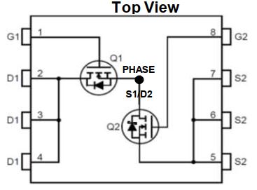
• Jak testować podwójne mosfety na zwarcie ?

#1 Jak testować podwójne mosfety na zwarcie ?


von patryk006 24 März 2020, 16:49
Dokładny model:
AON6994
http://www.aosmd.com/res/data_sheets/AON6994.pdf

Mosfet w układzie zasilania GPU, Czy niska oporność względem G1 a S2 to "norma" ?(ok. 15Ω)
Wszystkie cewki mają poprawne zasilanie (ok. 0.9V)

Jak mierzyć na przebicie tego typu mosfety ?

Re: Jak testować podwójne mosfety na zwarcie ?


von Google Adsense [BOT] 24 März 2020, 16:49

#2 Re: Jak testować podwójne mosfety na zwarcie ?  [GELÖST]


von matic 24 März 2020, 17:25
patryk006 hat geschrieben:Czy niska oporność względem G1 a S2 to "norma" ?(ok. 15Ω)
Hello!
No, this resistance should be in MΩ range. It is probably also low resistance between pin "G1" and "PHASE" (large pad on bottom side) and the same between pin "S2" and "PHASE".
In this case this transistor is bad and needs to be replaced.

patryk006 hat geschrieben:Jak mierzyć na przebicie tego typu mosfety ?
If you checked the data sheet for this transistor, you probably noticed that there are actually two MOS-FET transistors in single package. Treat it as two separate transistors (Q1 and Q2) and test each of it separately (like all other single MOS-FET transistors).

Bild

#3 Re: Jak testować podwójne mosfety na zwarcie ?


von patryk006 27 März 2020, 01:10
Thanks

Re: Jak testować podwójne mosfety na zwarcie ?


von Google Adsense [BOT] 27 März 2020, 01:10

Wer ist online?

Mitglieder in diesem Forum: 0 Mitglieder und 0 Gäste

_______________________________
Alle Rechte vorbehalten. Das unerlaubte Kopieren des Inhalts dieser Website oder eines Teils davon ist strengstens untersagt.
Alle auf dieser Website veröffentlichten Marken, Markennamen, Produkte oder Dienstleistungen gehören ihren gesetzlichen Eigentümern, sind urheberrechtlich geschützt und werden nur zu Informationszwecken verwendet.